
China turns to older chipmaking technology to make, smaller, faster 3nm chips
Chinese researchers have developed an early process for building gate-all-around (GAA) transistors at the sub-3nm...
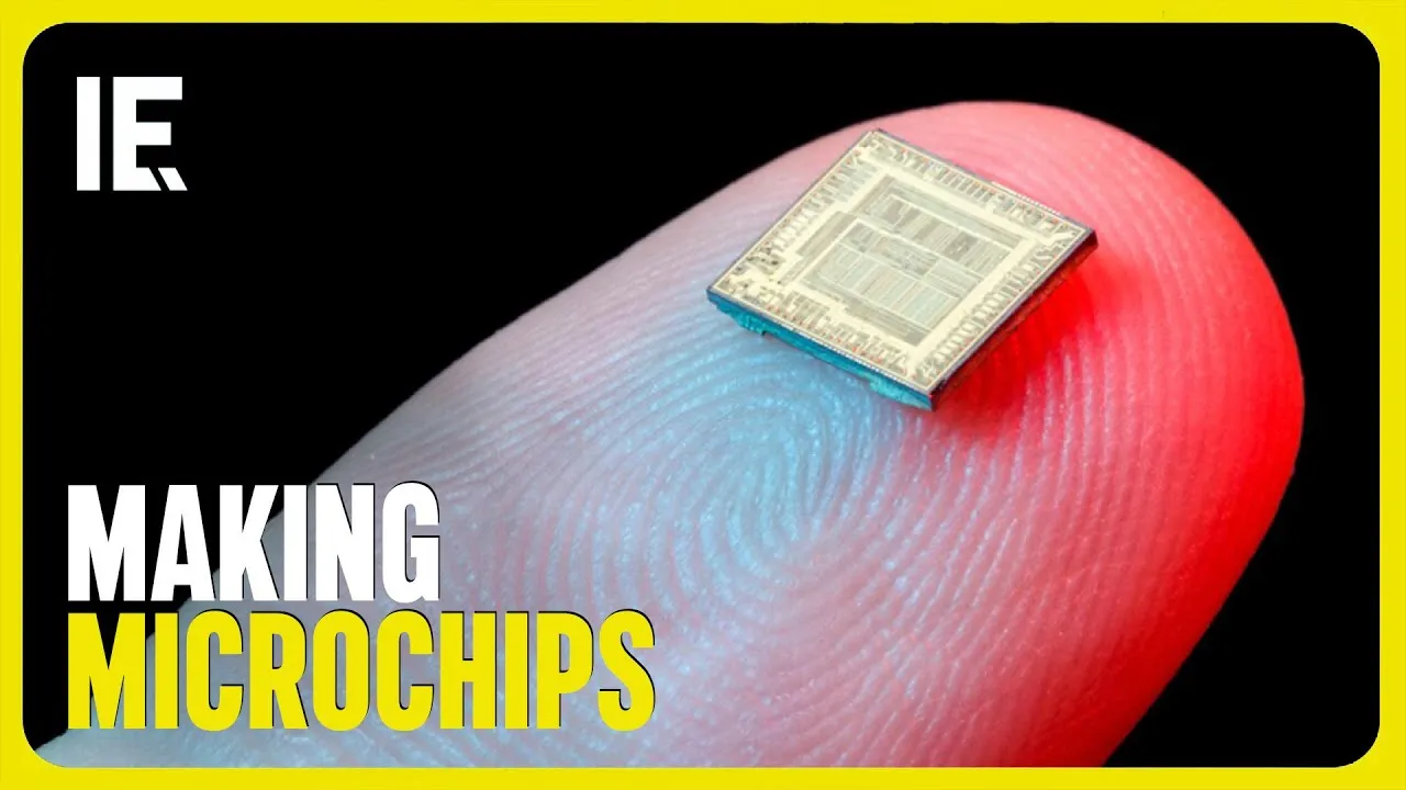
Chinese researchers have developed an early process for building gate-all-around (GAA) transistors at the sub-3nm level using deep ultraviolet (DUV) lithography, potentially offering China another route toward advanced chip manufacturing without access to the most advanced EUV machines.
The work, reported by Digitimes based on comments from veteran Chinese semiconductor researcher Ye Tianchun, comes as US and Dutch export restrictions continue to limit China’s access to ASML’s most advanced lithography systems.
The Chinese Academy of Sciences (CAS) says its researchers have completed early integration of stacked nanosheet-channel GAA CMOS transistors using DUV tools. However, the technology remains at an early development stage and has not demonstrated that it can support commercial-scale production.
GAA architecture could help overcome lithography limits
The research is focused on GAA transistors, an architecture that is replacing FinFET designs as semiconductor manufacturers move toward smaller process nodes. Unlike FinFETs, where the gate surrounds the transistor channel on three sides, GAA designs wrap the gate around the channel, providing greater control over the flow of current, the South China Morning Post reported.
The CAS team has reportedly integrated stacked nanosheet-channel GAA CMOS transistors using DUV lithography. Ye Tianchun, a veteran researcher from the Chinese Academy of Sciences’ Institute of Microelectronics, described the work as an early process route for developing sub-3nm devices.
However, that does not mean China has demonstrated a production-ready sub-3nm chip. The Chinese researcher emphasized that the work remains at an early stage and that further wafer-level validation will be needed to determine whether the process can eventually be transferred to a manufacturing line.
Still, the approach is significant because GAA technology is already being used by leading semiconductor manufacturers. Samsung began mass-producing 3nm chips using GAA, while TSMC moved to the architecture for its 2nm process in 2025.
Looking for ways around EUV restrictions
The research comes against the backdrop of China’s limited access to extreme ultraviolet (EUV) lithography, the technology used by leading chipmakers to manufacture the most advanced semiconductor nodes. ASML’s EUV machines use 13.5nm light to pattern extremely small features on silicon wafers. The systems are among the most sophisticated industrial machines ever built and are critical to modern leading-edge chip production.
Export restrictions prevent ASML from selling EUV systems to Chinese customers and as a result, Chinese semiconductor researchers have increasingly explored ways to extract more performance from older DUV equipment, including through new transistor structures, process techniques and materials.
CAS has been working on several pieces of this puzzle. In 2025, researchers at the institute developed an all-solid-state DUV laser capable of producing 193nm coherent light, the wavelength used by advanced DUV lithography systems. Furthermore, researchers are also investigating whether different device architectures and process techniques can compensate for limitations in lithography.
China’s semiconductor industry is nevertheless pursuing several parallel approaches. Huawei unveiled what it calls the Tau Scaling Law in 2026, a chip-design approach based on “time scaling” that the company says could eventually produce transistor densities comparable to a 1.4nm process by 2031.
Related articles

China fears US deployment of space weapons raises risks of fresh arms race: Report
The United States has publicly acknowledged that it has weapons deployed in orbit, marking a...

Trump wants ‘AI Force’ to keep US AI race moving, push ahead with modern tech despite concerns
President Donald Trump says he plans to create an “AI Force” and appoint a new...

Scientists transport 92 antiprotons by road for first time, store them in vessel for over a month
Scientists succeeded in transporting antiprotons by road for the first time in a purpose-built trap...

A mathematical rule against disagreement survives beyond quantum mechanics
Two people can examine the same evidence and reach different conclusions. However, if they share...
Volkswagen electric bus sets Guinness World Record, drives 62,000 miles across 92 countries
A Volkswagen ID. Buzz has completed a 99,767-kilometer (roughly 62,000 miles) journey through 92 countries...

Low-cost US interceptor destroys drones without jamming their signals
A US defense startup has tested a low-cost interceptor missile designed to physically destroy small...