
Oxygen-based chipmaking method controls 2D crystal growth with over 99% success
Researchers in South Korea have developed a semiconductor manufacturing technique that controls where individual crystals...
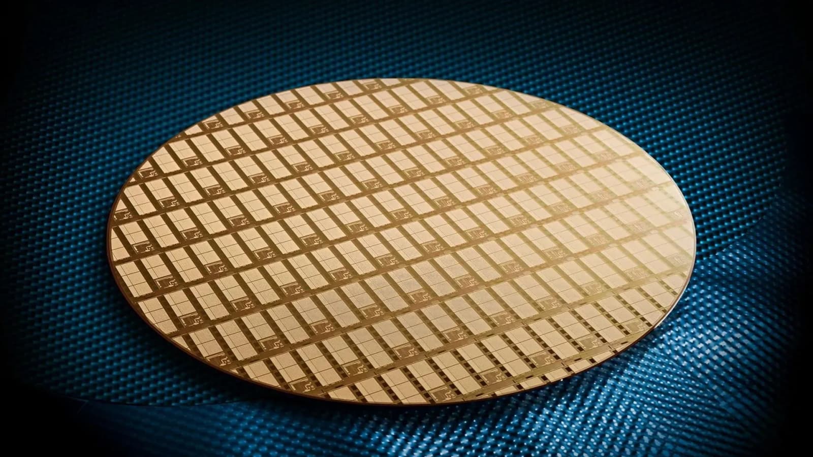
Researchers in South Korea have developed a semiconductor manufacturing technique that controls where individual crystals form with more than 99% success across 400 patterned growth regions, potentially helping manufacturers build vertically stacked computing chips.
The technique allows researchers to grow a single crystal of molybdenum disulfide (MoS₂), a semiconductor only a few atomic layers thick, at a predetermined position instead of allowing multiple crystals to form randomly.
A team led by the Korea Advanced Institute of Science and Technology (KAIST), working with UNIST, Hanyang University and TDS Innovation, developed the method using oxygen released from an oxide barrier to control where crystal growth begins.
The researchers say the approach could address a major obstacle in manufacturing stacked chips, where semiconductor layers must be formed precisely on top of existing circuits without introducing defects that affect performance.
Oxygen controls crystal formation
Conventional semiconductor growth methods can define the general area where a thin film forms, but controlling the exact starting point of each crystal remains difficult.
When several crystals grow independently and meet, they create grain boundaries. These boundaries disrupt the regular arrangement of atoms and can interfere with the movement of electrons through the semiconductor.
The researchers developed a process called etching-flux-mediated single-centered nucleation (EF-SCN). Nucleation is the initial stage of crystal formation, when atoms begin arranging themselves into an ordered structure.
The process uses an oxide barrier, such as hafnium oxide (HfO₂), surrounding the designated growth region. Oxygen released from the barrier acts as an etching agent, suppressing unwanted crystal formation.
The oxygen’s effect is strongest near the edges of the patterned region and gradually weakens toward the center.
This creates conditions that favor crystal formation at a single central point. Once growth begins there, the process also suppresses additional crystals from forming nearby.
Using this method, the researchers successfully grew individual MoS₂ crystals at designated central positions in more than 99% of 400 patterns.
The team also demonstrated selective metal deposition using structures combining molybdenum disulfide and molybdenum diselenide (MoSe₂).
In these structures, a thin ruthenium metal film formed selectively on the MoSe₂ regions, demonstrating another way to control material placement during semiconductor fabrication.
Stacked chips move closer
Two-dimensional semiconductors are being investigated for future chips because they retain semiconductor properties despite being only a few atomic layers thick.
Their small thickness could allow manufacturers to stack computing and memory components vertically, reducing the distance data travels between them.
Moving data within a chip consumes energy and contributes to processing delays. Placing components closer together could reduce those costs, particularly in systems handling large computational workloads.
However, producing such chips requires precise control over semiconductor growth on surfaces containing previously fabricated circuits.
The KAIST technique offers a possible way to grow high-quality 2D materials directly at designated locations, avoiding the need to manufacture them separately and transfer them onto a chip.
The researchers examined the mechanism through growth experiments and simulations, but they have not demonstrated a complete stacked processor or measured improvements in computing speed or energy consumption.
The findings establish control over crystal nucleation rather than commercial chip performance. Further development would be needed to determine whether the method can be integrated into semiconductor manufacturing at scale.
The study was published October 8 in Nature.
Related articles

Tiny chip stores memories in flowing water without conventional electronics
Yale researchers have found a way to make flowing fluids remember what happened before, using...

Meta releases Muse Wonder, its first frontier model for personal and professional agents
Meta’s Superintelligence Lab launched Muse Wonder and Muse Wonder Full, its first frontier-class models, emphasizing Active Memory and long-running agent work. Wonder is available via the Meta Model API and Muse Code; Wonder Full is limited to Muse Code subscribers.

Anthropic to share first Q3 figures with investors as it prepares for a possible record IPO
CNBC reports Anthropic will disclose third-quarter financials for the first time to institutional investors meeting at its San Francisco headquarters this week, as the AI lab prepares for what could be a roughly $2 trillion IPO.

Reuters: OpenAI and Anthropic sought control over what outside AI safety evaluators can publish
According to Reuters, OpenAI and Anthropic pushed for significant control over outside evaluators’ publications over trade-secret concerns, even after publicly endorsing editorial independence. Talks have shifted in recent days, and both labs dispute parts of the characterization.

OpenAI and Anthropic tell UK lawmakers voluntary AI pledges are not enough
At a UK parliamentary hearing, OpenAI and Anthropic backed a statutory AI safety framework, saying voluntary commitments are not a durable plan for frontier risk. Google DeepMind and Meta declined to support new legislation, deepening a public split among labs.

Google DeepMind launches Gemini 4 Argon globally for coding, science and cyber defense workloads
Google on October 13, 2026 made Gemini 4 Argon available worldwide via the Gemini API, the Gemini app and Antigravity. The frontier model ships with a 1M-token unified context window and introductory API pricing of $2 per million input tokens and $10 per million output tokens.