
Silicon photonic chips gain multiple light functions with ultrathin crystal films
Researchers at Washington University have developed a new method to let silicon photonics efficiently perform...
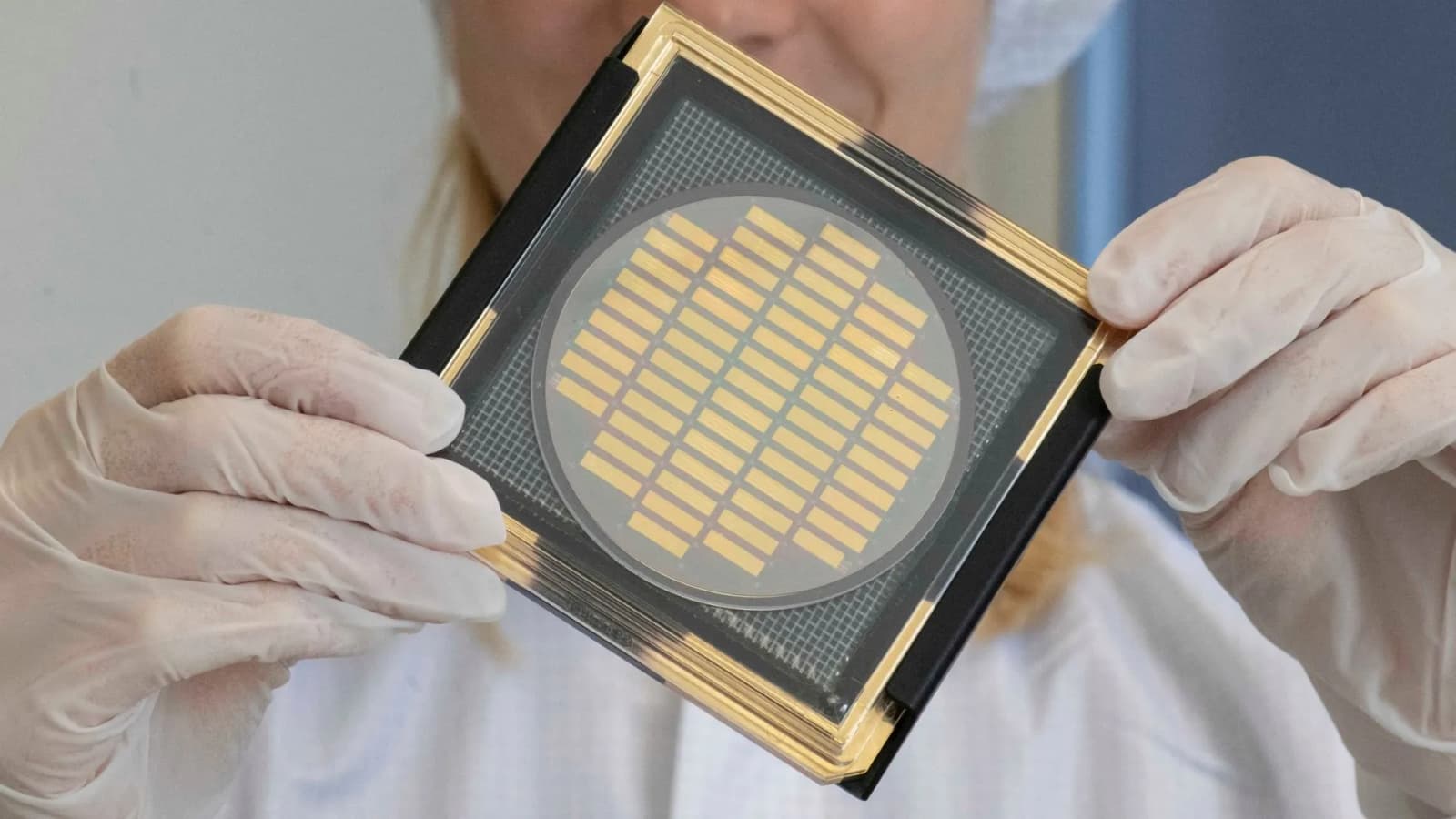
Researchers at Washington University have developed a new method to let silicon photonics efficiently perform the optical functions needed to control and detect light, overcoming a key materials limitation that has restricted their capabilities.
The team at the McKelvey School of Engineering in St. Louis added ultrathin, single-crystal films to existing silicon photonic circuits, with different crystalline materials providing specific functions such as controlling, modulating, and detecting light.
Until now, adding such materials has been difficult because growing them directly on silicon can create compatibility and manufacturing problems. The new method instead grows the crystals separately and transfers them onto the chip afterward.
The materials can be placed side by side or stacked depending on the function required. The team demonstrated light modulation and control, as well as detection across wavelengths ranging from ultraviolet to near-infrared, describing the modular approach as “photonic Legos.”
Crystals add new functions
The team used four materials with different properties to demonstrate the framework. Single-crystalline barium titanate (BTO) provided electro-optic modulation, allowing electrical signals to control light traveling through a chip.
For nonreciprocal light control, the researchers used cobalt ferrite (CFO), which can control how light travels through a device. They also integrated gallium arsenide and gallium nitride membranes on silicon nitride to detect selected wavelengths spanning ultraviolet to near-infrared light.
The researchers went a step further by stacking BTO and CFO nanomembranes on silicon micro-ring resonators, allowing a single device to control light using both electrical and magnetic effects.
“We developed a manufacturing process that will give us more freedom to design these new photonic chips,” said Sang-Hoon Bae, an assistant professor of mechanical engineering and materials science at the university.
Building beyond silicon limits
Photonic integrated circuits use light to move and process information instead of relying solely on electrical signals. Because photons can carry large amounts of data quickly while reducing some of the power and heat demands associated with electronic data transfer, photonic chips are being explored for faster computing and communications.
The technology could become particularly useful as data centers and computing systems handle growing workloads. Researchers are developing photonic chips for high-speed optical communications, photonic computing and co-packaged optics, as well as more specialized applications in sensing and quantum technologies.
Silicon photonics already benefits from decades of advances in semiconductor manufacturing. The challenge has been adding materials that can perform functions silicon cannot while still taking advantage of existing silicon chip technology.
“Each material brings its own strengths,” said Lan Yang, a professor of electrical and systems engineering at Washington University. “By growing high-quality crystals separately and then bringing them onto an existing photonic circuit, we gain more freedom to choose the material for the function we need.”
The researchers said the modular approach could eventually allow chip designers to select and combine different crystalline membranes based on the functions a particular application requires. The current work demonstrates the integration framework and several optical functions, rather than a complete commercial photonic processor.
The research was published in Nature.
Related articles

38-ton combat vehicle’s systems to be controlled by voice, deliver more battle power
A new deal signed between two defense companies is set to bring human machine teaming...

New counter-drone weapon uses 4D radar to track threats over 800 meters while moving
EOS Defense Systems USA is developing a new Slinger counter-drone system with upgraded sensors and...

Teenage Engineering’s CEO says it’ll stop making synths
Teenage Engineering founder and CEO Jesper Kouthoofd told Highsnobiety that it plans to stop making synths. And yes, that includes the iconic OP-1, which put the company on the map.

We found some great October Prime Day deals under $50
Getting in on the Prime Day action doesn’t have to result in an empty wallet.

Android’s physical navigation buttons are back on Googlebooks, but not the way you think
A common misconception I've seen with Googlebooks is that the Quick Insert and Google logo keys are new. They're not, as they first debuted a couple of years ago on some Chromebooks.

New heat pump tested at 320°F could help factories ditch fossil fuels for steam
Researchers have tested high-temperature heat pumps at 320 degrees Fahrenheit and showed that the technology...