
‘Camera’ captures atomic shockwaves before quantum bit forms inside a crystal
Scientists have recorded what happens inside a crystal in the split second before a quantum...
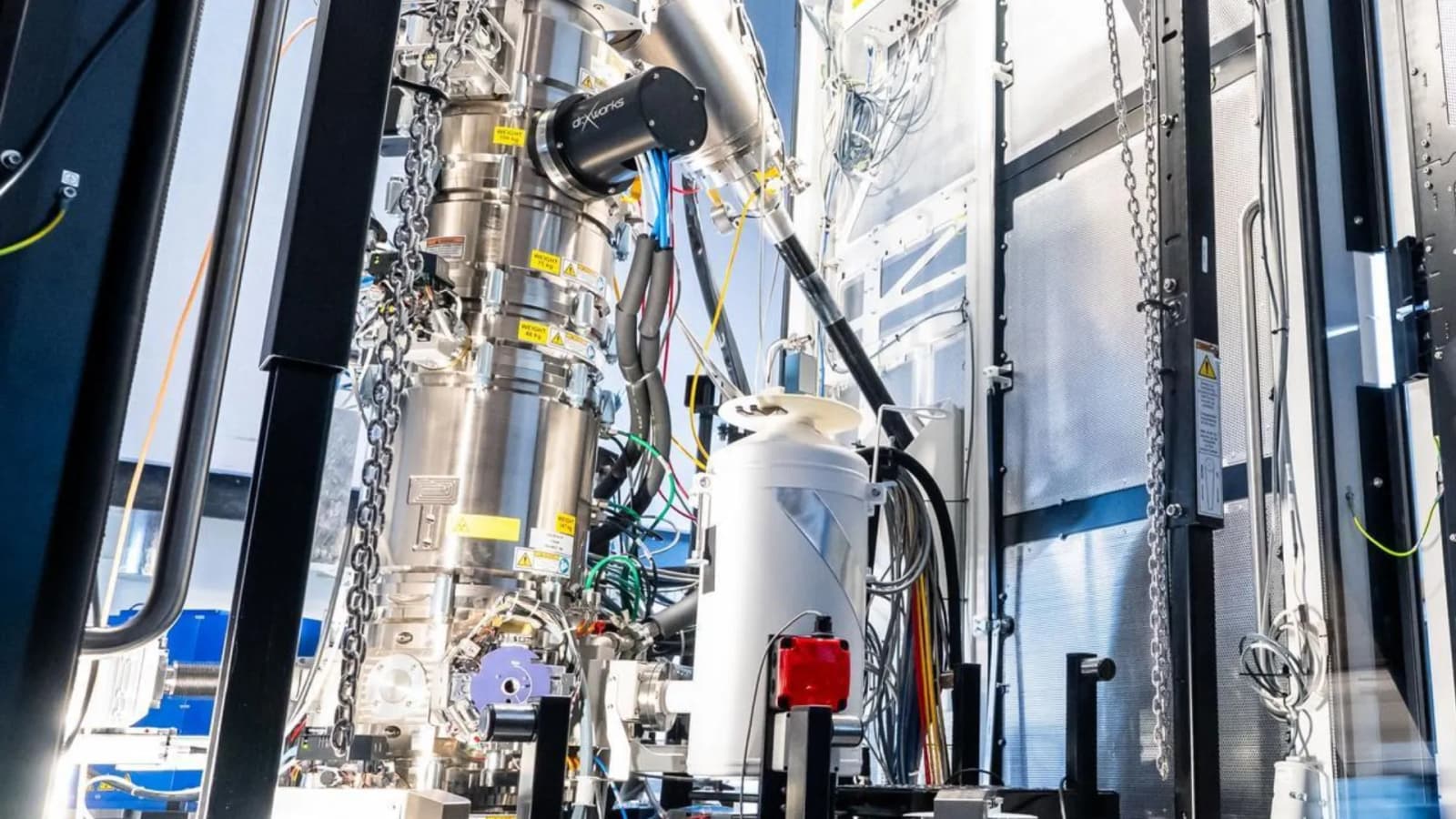
Scientists have recorded what happens inside a crystal in the split second before a quantum bit forms. A team at the US Department of Energy’s Argonne National Laboratory tracked structural changes within silicon carbide in three dimensions.
They used one of the world’s most powerful X-ray sources for the experiment. Their findings, published in the journal ACS Nano, allow researchers to watch how a material’s atomic lattice responds to laser strikes beneath the surface in real time.
Building a solid-state quantum device often involves deliberate damage. Physicists fire a blindingly fast laser pulse into a crystal lattice. The flash lasts only a fraction of a picosecond, and the beam knocks individual atoms out of place. This process leaves behind tiny empty spaces known as vacancies.
“Far from being flaws, these vacancies can behave as qubits — the fundamental building blocks of quantum information,” noted the ANL. Qubits hold and process quantum information. For that reason, they serve as the basic building blocks for quantum computers, secure communication networks, and advanced medical sensors.
A game of trial and error
Until now, the exact physics of this laser strike remained a blind spot. Older methods used beams of ions or electrons, but they offered little control over position. Lasers can target specific spots, but researchers could only guess how energy moved through the lattice. Creating qubits was largely a game of trial and error.
“Before you can precisely engineer quantum defects, you have to understand exactly what the laser is doing inside the material,” said Argonne scientist Haidan Wen, an author of the paper.
“This technique lets us watch that process unfold, especially how atoms move in ways that weren’t possible before.”
To solve the puzzle, the Argonne team built an atomic-scale camera. They combined an ultrafast laser with the laboratory’s Advanced Photon Source, which produces exceptionally bright X-ray beams. The team focused this beam down to several hundred nanometres, which is roughly one hundred times thinner than a human hair.
Hard X-rays pass straight through the crystal. Because of this penetration, the pulses recorded activity deep inside the sample, rather than just on the outer surface. The laser struck the material, and synchronized X-ray flashes captured the immediate aftermath.
Revealing two distinct reactions
The images revealed two distinct physical reactions occurring side by side. Part of the energy surges through the crystal as an organized shockwave. This wave behaves like ripples spreading across a struck rubber sheet. Meanwhile, the rest of the energy spreads out more slowly as heat. This thermal burst causes nearby atoms to vibrate randomly before the lattice settles down again.
Silicon carbide is already a cornerstone of the commercial computer chip industry. Factories already know how to manufacture it on a massive scale. As a result, the material is widely viewed as a top candidate for mass-producing quantum hardware.
Engineers hope this data will reduce the need for guesswork. By mapping this energy transfer, researchers aim to eventually place individual qubits at precise coordinates on demand.
The team now plans to test their imaging method on other quantum materials, bringing lab-grown prototypes closer to factory assembly lines.
Related articles

Nobel Prize in Chemistry awarded to two scientists for providing solution to a century-old mystery
The Nobel Prize in Chemistry 2026 awarded to two scientists for providing a solution to...
Smart US tool could cut quantum device tuning time in hunt for elusive dark matter
Scientists in the US have been developing a smart agent that could automatically tune sensitive...
Microscopic nuclear fuel particles from Chernobyl still intact after 40 years
Forty years after explosions scattered radioactive debris from Chernobyl’s reactor across the surrounding landscape, some...
Wave-shaped building walls and roofs can cut hurricane wind pressure by up to 60%: study
Buildings with wave-shaped exterior walls and roofs can withstand hurricane-force winds far better than conventional...

Heat first, compress later: New fusion strategy flips the script to reach ignition
A tiny amount of tungsten inside fusion plasma could roughly double the pressure needed to...

Google’s power-hungry data centers crave nuclear energy
Google announced a new agreement to update six nuclear power plant sites across the US as the tech giant seeks to generate more electricity for its power-hungry data centers.