
US scientists find 7-volt switch can strain sapphire thousands of times its depth
Researchers in the US have recently discovered that a 7-volt pulse applied to an ultra-thin...
Researchers in the US have recently discovered that a 7-volt pulse applied to an ultra-thin electronic film could cause structural changes deep inside the sapphire supporting it.
Scientists at the US Department of Energy’s (DOE) Argonne National Laboratory (ANL) found out that the effect extended tens of micrometers into the sapphire, thousands of times deeper than the thickness of the film itself.
Zahir Islam, PhD, a physicist at ANL, and co-author of the study, said the finding challenges a common assumption in microelectronics that the substrate beneath a thin film simply acts as a passive support. Instead, sapphire can respond when the electronic device operates and influence the behavior of the film above it.
“This is a potentially paradigm-shifting observation,” Islam stressed. “You cannot simply assume that the substrate has nothing to do with a device’s properties or behavior.”
Film strains sapphire
For the study, the researchers examined vanadium dioxide (VO2) films, which are grown on sapphire. It can switch from an electrical insulator to a conductor when a voltage is applied.
Vanadium dioxide is often used in electronic switches, wireless devices, adjustable optical systems, and smart windows. The material is also being explored for use in memristors, electronic components that can retain data about previous electrical signals.
This makes them attractive for neuromorphic, or brain-inspired, computing. In the device studied by the scientists, applying a voltage triggered a localized transition from an insulator to a conductor. This generated a narrow conducting filament inside the insulating film.
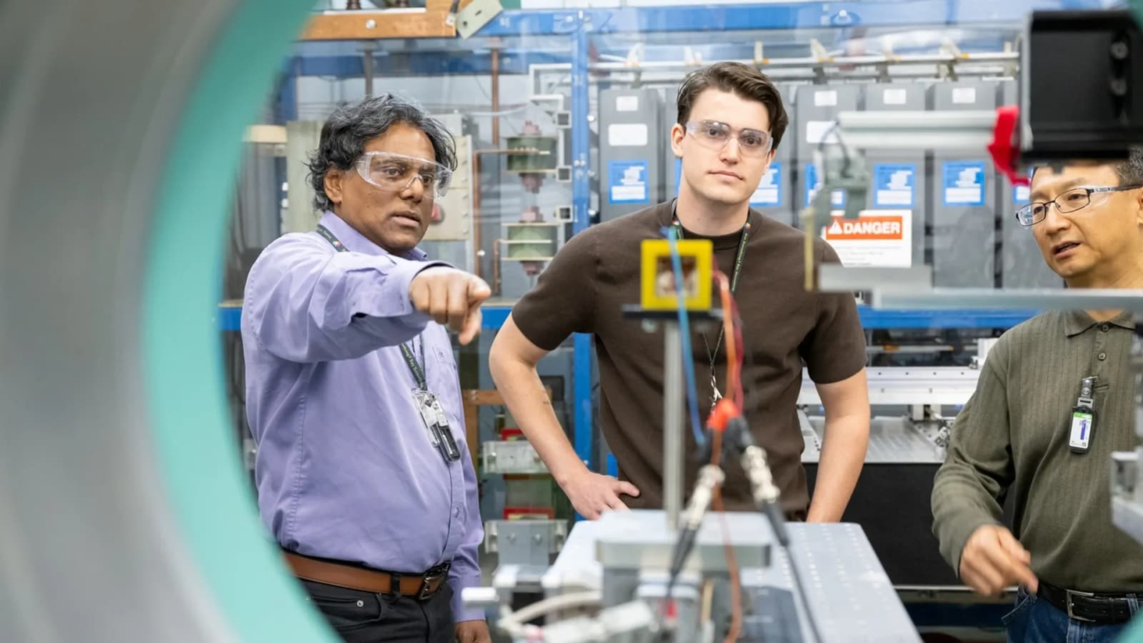
APS scientists (from left) Zahir Islam, Elliot Kisiel and Zhan Zhang at beamline 6-ID-B of the APS. Credit: Mark Lopez / Argonne National Laboratory
The device also remembered when it had been activated before. This allowed it to switch again at a lower voltage. To investigate what happened during the process, the team used dark-field X-ray microscopy at Argonne’s Advanced Photon Source (APS). The method allowed them to examine structural changes across the device and deep beneath its surface.
They discovered that the conducting filament expanded as the voltage increased. It also produced uneven strain in the sapphire below. The distortion reached tens of micrometers into the rigid substrate and was far greater than what they expected from heating alone.
Future electronic devices
Elliot Kisiel, PhD, a Maria Goeppert Mayer fellow at ANL, as well as lead author of the study, stated that the team initially suspected the unexpected response in the sapphire substrate was an experimental artifact. An experimental artifact is a false or misleading result caused by the experiment itself rather than the phenomenon being studied.
“Because the result was so surprising, we tested it over and over across multiple devices, samples, film thicknesses and even different substrates,” Kisiel explained in a press statement. “The effect held up.”
Kisiel is certain the finding could become more important as electronics shrink and more components are packed closer together. For instance, activity in one device could cause mechanical changes in a shared substrate that affect nearby devices.
While this could create problems, it could also be harnessed for neuromorphic computing, where interconnected devices mimic the way the brain processes information. “The brilliance of the APS really shined to bring this work to the finish line,” Islam concluded. “We were able to study many more devices in far shorter beam time and capture rich structural information with high fidelity.”
The study has been published in the journal Science.
Related articles

Ultra-high-power lasers open new pathways for non-destructive material inspection
Superman’s X-ray vision isn’t actually that super. X-rays work well for seeing through thin objects...
CERN researchers report first observation of differences in nucleons within the atom
Researchers at the ATLAS Collaboration at the CERN have found the origins of an observation...
US scientists turn 95% calcium-rich eggshell waste into stronger magnesium alloys
U.S. researchers have demonstrated a way to turn powdered eggshells into stronger, harder magnesium alloys,...