
38,000-sq-ft Wisconsin facility unites eight labs for next-gen semiconductor materials
EMD Electronics, the North American electronics business of Germany’s Merck KGaA, has opened a 38,000-square-foot...
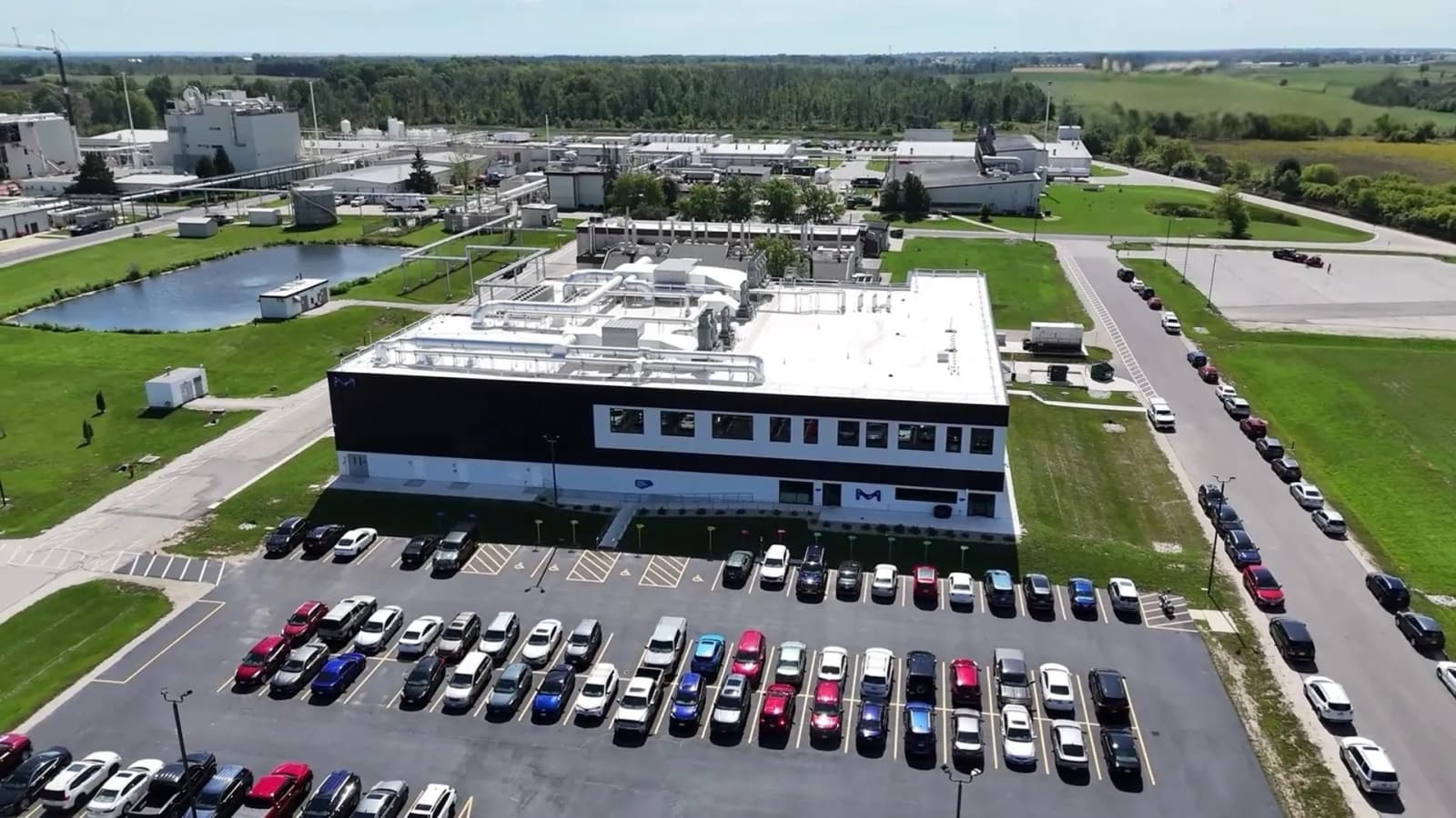
EMD Electronics, the North American electronics business of Germany’s Merck KGaA, has opened a 38,000-square-foot research center in Wisconsin with eight laboratories designed to develop materials for next-generation semiconductor manufacturing.
The Sheboygan Falls facility is part of a $200 million multi-year U.S. investment covering semiconductor operations in Wisconsin, California and Oklahoma. Another expansion at the Wisconsin site is scheduled for completion in 2027.
The new center brings material synthesis, development, scale-up and technology transfer into one location. EMD says the setup is designed to shorten the process of moving new materials from laboratory development toward customer testing and eventual commercial production.
Advanced chips increasingly rely on specialized materials and chemical processes as manufacturers pack more components into smaller spaces and adopt more complex device designs. EMD supplies the semiconductor industry with products including specialty gases, deposition materials, planarization chemicals and patterning materials.
Eight labs tackle scaling
The facility’s eight purpose-built laboratories cover different stages of the product development cycle, including discovery, development, qualification, analytical development, purification, packaging and hazard testing.
Bringing those functions together could allow researchers to develop a material, determine how to manufacture it at larger volumes and prepare the production process for transfer without relying on separate facilities. EMD says this will also allow it to work more closely with semiconductor customers as their manufacturing requirements change.
“The semiconductor industry is entering a period where integrated workflow solutions play a defining role in enabling the next generation of devices, particularly as AI drives increasing complexity and performance requirements,” said Bing Han, executive vice president and head of Thin Films at EMD Electronics.
“Materials innovation remains at the core of that transformation, but success increasingly depends on combining materials discovery, process expertise, and scale-up capabilities,” Han added.
We’re opening our new 38,000-sq.-ft. R&D facility in Sheboygan Falls, #Wisconsin, to accelerate advanced #semiconductor materials innovation—from discovery to qualification, faster.
Watch the full video & learn more: https://t.co/bnASF3MtBK#MaterialsScience pic.twitter.com/4lLa8K97wV
— EMD Electronics (@EMD_Electronics) October 5, 2026
The Wisconsin Economic Development Corporation is working with EMD Electronics on the expansion, which the state agency says will support skilled jobs and strengthen Wisconsin’s semiconductor industry presence. The announcement did not specify how many jobs the new facility will create.
Broader US expansion continues
The Sheboygan Falls project forms part of EMD Electronics’ wider effort to expand semiconductor research and manufacturing capabilities in the United States.
Its $200 million multi-year program also includes recently completed projects in Carlsbad, California, and Catoosa, Oklahoma, alongside the additional Wisconsin expansion planned for 2027.
That spending, in turn, sits within a larger $1 billion, five-year U.S. investment program announced by the company in 2021 to expand its research and manufacturing operations.
EMD also designed the new Wisconsin laboratories to reduce their environmental footprint. The company says the facility is powered by renewable energy and is targeting LEED Gold certification, although the certification has not yet been awarded.
For chipmakers, the practical focus of the new center is on reducing the gap between finding a promising material and proving that it can be reliably manufactured at the scale and quality required for semiconductor production.
Source: https://interestingengineering.com/innovation/emd-electronics-wisconsin-chip-materials-lab
Related articles

OpenAI is adding text watermarking in ChatGPT and Codex
An invisible, machine-readable watermark in text output is rolling out to ChatGPT and Codex, but only for users in the European Union at first.

Sam Altman says ‘some bad things’ will happen but AI is totally worth it
Sam Altman thinks that the benefits of AI will be so great that "the world should accept some bad things happening" along the way.

OpenAI PR tells journalist to ‘move on’ while asking Sam Altman about a ChatGPT user’s suicide
An OpenAI publicist tried to change the topic of CEO Sam Altman's interview with Vanity Fair's Mark Guiducci after the editor brought up a ChatGPT user's suicide.

Video: Robot hand performs magic tricks with precision using 20 independent joints
Chinese robotics startup LinkerBot has demonstrated the dexterity of its new robotic hand by teaching...

Humanoids to tackle bomb scenes, hazmat threats and prison searches
Singapore plans to deploy AI-powered humanoid robots alongside public safety officers by 2028, expanding the...

Apple’s new M6 Mac Mini is over $100 off
Really the only negative associated with the new M6-powered Mac Mini is its high price.